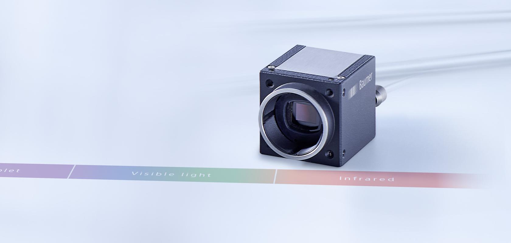
Short-wave infrared (SWIR) is a part of the electromagnetic spectrum that lies just beyond the visible range of light. It typically refers to the wavelength band of light between 900 and 2500nm.
SWIR technology has traditionally been leveraged in more specialised applications due to its ability to see beyond the visible spectrum, offering unique imaging solutions where traditional cameras may fall short. Some of these applications include semiconductor inspection, to identify defects that might be invisible under normal light; moisture detection in pipes or food production; and inspecting objects under a surface, such as in packaging.
More recently, SWIR has been making its way into the broader machine vision market, driven by advancements in sensor technology, with innovations such as the new Sony SenSWIR sensors, which were designed to provide enhanced image quality, compact designs, and reduced costs.

Torsten Wehner, Product Manager at Baumer Group (pictured above), explains: “In addition to the combination of the visual range up to the SWIR range, the achievable image quality is significantly better compared to previous InGaAs sensors. This is especially true for the resulting defect pixels and image noise. With the SenSWIR technology, Peltier cooling (TEC) can be avoided in many applications. This makes the cameras significantly cheaper and more compact in design.”
Transitioning to SWIR: The challenges
However, transitioning SWIR technology to a broader market comes with its own set of challenges. Companies and organisations using industrial cameras often need to navigate issues related to image quality, camera size, power consumption, and defect pixels. Wehner says: “The challenge for our customers is to understand how image quality can be influenced by which measures in order to achieve the best possible, most stable result in imaging processing. InGaAs technology is not as widespread yet, and the technologies required to manufacture it are different from the familiar silicon-based manufacturing process. Silicon-based CMOS technology also took many years to achieve the image quality we know today. The first images from CMOS sensors had very similar characteristics to today’s InGaAs sensors, which are a huge step forward in terms of image quality with SenSWIR technology, but are not yet at the same level as silicon-based CMOS sensors. A key issue is the temperature of the image sensor. The warmer it gets, the more defect pixels appear. Each additional defect pixel can make the subsequent image processing more unstable. Further corrections in the camera will not help.”
Baumer has developed several key components to address the issue of defect pixels, focusing on temperature management and advanced correction methods. The design of the camera housing plays a critical role in dissipating heat generated by the electronics, thus reducing the number of defect pixels. Wehner explains, "Our first priority is to create as few defect pixels as possible, which is why we emphasise effective heat dissipation and low power consumption in our camera designs."
The solutions to defect pixels
A key feature is the company’s patented thermal housing design, which incorporates a cooling fin and an integrated cooling pipe that can be used for active cooling. This approach can not only help to reduce the temperature of the image sensor, but also protect the optics from thermal expansion, to ensure high measurement accuracy. Says Wehner: “This is a significant difference from other cooling options, which are usually attached to the camera as an additional unit. We are better at temperature management, we benefit directly from the compact size, where other cooling solutions always require more installation space, and we save money on inventory or procurement because no additional equipment is needed.”
As well as physical design improvements, Baumer implements both static and dynamic defect pixel correction methods in their camera firmware. Static correction uses a predetermined list of defect pixel coordinates, offsetting them against neighbouring pixels. Dynamic correction adjusts for defects detected during image acquisition, ensuring stable and high-quality images. Wehner explains: “These two correction methods work together to provide the best possible image quality for our customers' image processing needs.”
Baumer also prides itself on ensuring transparency by giving customers full control over the defect pixel correction settings. Users can disable these functions if necessary and have access to all settings for documentation and further customisation. “For example,” explains Wehner, “for some customers it is very important to know which pixels are being corrected. They can read the vectors of the pixels from the list and save them, for example as documentation. The list can also be extended by the customers themselves, or they can store their own measurements of the defect pixels in the list. However, we assume that most customers use our corrections and are very satisfied with them.”
Applications across various industries
Baumer’s SWIR cameras are already making a significant impact in industries such as semiconductor manufacturing, food inspection, and pharmaceuticals. Wehner reveals: “In semiconductor manufacture the focus is on ‘high precision’ and ‘best image quality’ at the best possible price/performance ratio. With SWIR technology, a silicon wafer becomes transparent and shows its inner structure. In the food industry, the opposite is sometimes true. Transparent water becomes opaque and forms a clear contrast to its surroundings. This makes it easy to detect fill levels in non-transparent bottles or to inspect differences in the moisture content of food. In the pharmaceutical sector, for example, packaging can be made translucent to enable a completeness check of pills after the packaging has been sealed. It will be very exciting to see what other ideas our customers come up with in the future.”
Speaking of the future, with technology developing at pace, there is no laurel resting for Baumer. Wehner explains: “Higher resolutions will be in demand in the future. Sony already has sensors that enable 3 and 5 megapixel resolutions. We will integrate these resolutions into our cameras and continue to support our customers. We believe that there is a wide range of applications here that cannot be realised with ‘normal’ sensors. With the portfolio from 0.3 to 5 megapixels, the applications will expand considerably. Our new SWIR cameras can allow applications to be solved that in the past would certainly have failed due to the price of the available SWIR cameras. The new SWIR image quality and the higher resolutions at a very good price/performance ratio now allow a solution in a wider range of applications.”